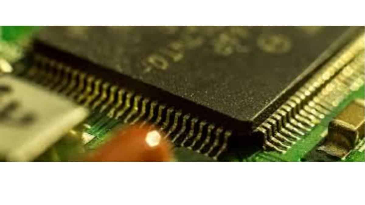
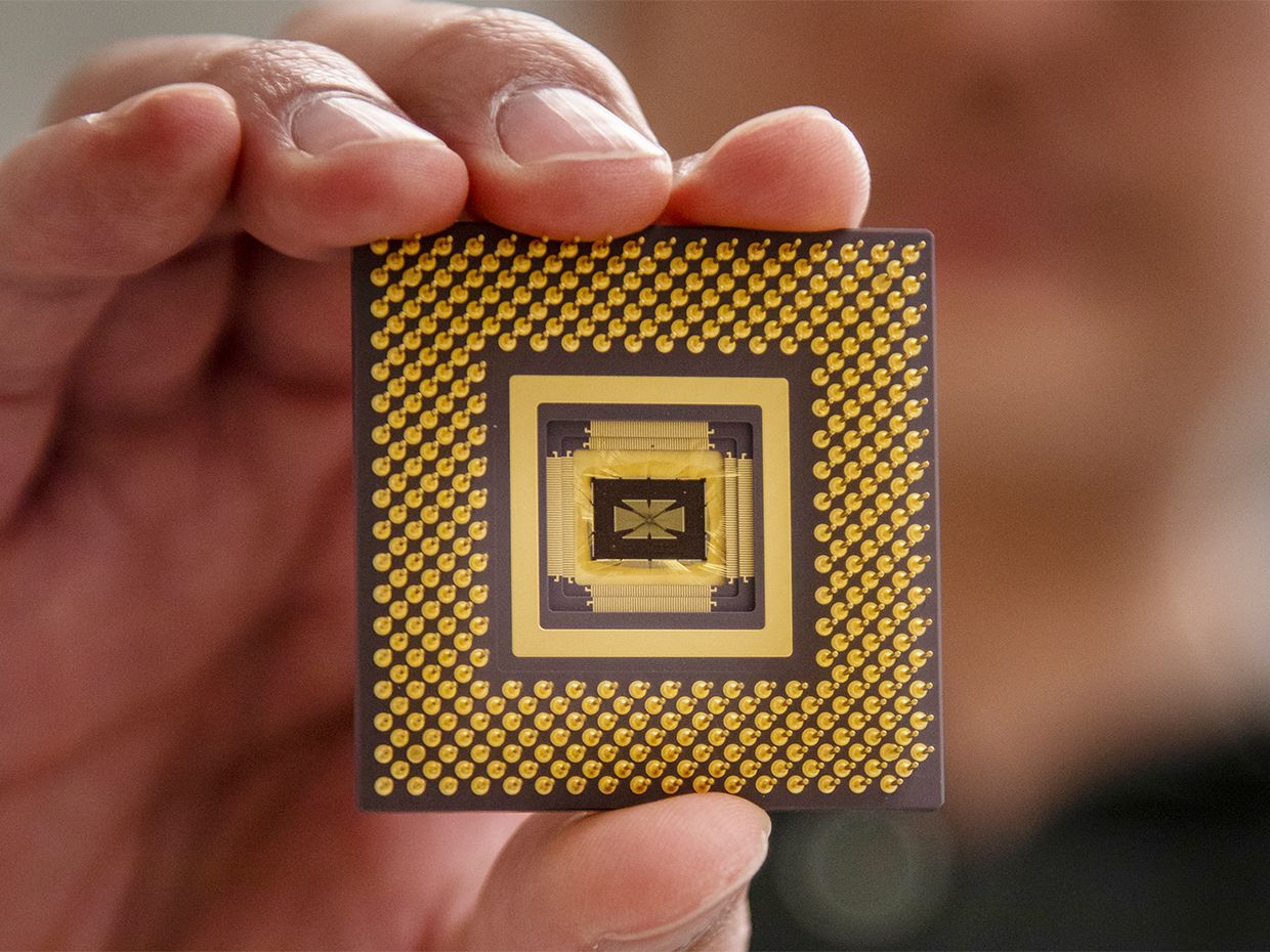
In a step towards advancement which may lead to faster, smaller, and more energy-efficient electronic chips for consumer electronics and brain-inspired computing, the scientists from the University of Texas at Austin, have created the smallest memory device yet.
Researchers in the US also found out the physics behind it that unlocks the dense memory storage capabilities for these tiny devices.

In the journal Nature Nanotechnology a recently published research states that, the scientists reduced the size of the thinnest memory storage device then, and shrunk the cross section area down to just a single square nanometre.
According to the researchers, they were only able to make the devices much smaller after getting a handle on the physics of the pack dense memory storage capability of these devices. They said that the key to unlocking the high-density memory storage capability was the ultrasmall holes in the material provided.
Deji Akinwande, a co-author of the study explained, “When a single additional metal atom goes into that nanoscale hole and fills it, it confers some of its conductivity into the material, and this leads to a change or memory effect.”
Though the primary nanomaterial used in their study is a compound molybdenum disulfide also known as MoS2, the researchers believe that the discovery could apply to hundreds of related atomically thin materials.
They said that smaller processors enable manufacturers to make more compact computers and phones and that shrinking down chips also decrease their energy demands and increase capacity. This means faster and smarter devices that take less power to operate, the scientists explained.
At the time the thinnest memory storage device ever recorded, with a single atomic layer of thickness was “atomristor” as dubbed by the researchers. Also, shrinking the memory device is not just about making it thinner but also building it with a smaller cross-sectional area, they added.
“The scientific holy grail for scaling is going down to a level where a single atom controls the memory function, and this is what we accomplished in the new study,” Akinwande said.
This new device now falls under the category of memristors. Memristors is an area of memory research which is centred around electrical components having the ability to modify resistance between its two terminals without a need for a third terminal in the middle.
Researchers say these devices can be smaller than most currently used memory devices and also boast more storage capacity.
They added that the new memristor promises a capacity of about 25 terabits per square centimetre, which is about 100 times higher memory density per layer compared with commercially available flash memory devices.