A printed circuit board (PCB) that fails electromagnetic interference (EMI) testing or comes back from the fabrication facility with a stack of design rule violations doesn’t fail at the bench. It fails at the design stage. The tools you choose and the discipline you bring to the layout process determine whether a board makes it to production or goes back to square one. It all starts with knowing how to design a PCB the right way from the very start. We drew on insights from EMSG Inc. to put together this guide.
The Core Principles of DRC and EMI in PCB Design
Passing a design rule check (DRC) and minimizing EMI are the two objectives that dominate every serious PCB layout effort. Both are achievable, but each requires a clear understanding of what you’re working toward.
Understanding Clean DRC
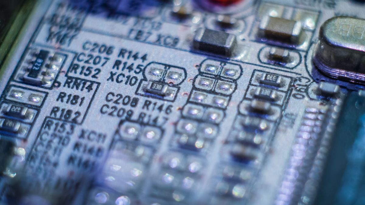
A DRC, an automated function built into PCB layout software, verifies whether a design meets the manufacturing constraints of a specific fabrication house. These constraints include minimum trace widths, spacing between conductors, drill hole sizes and solder mask clearances. Catching violations early prevents costly respins and keeps yield rates high. An error-free DRC output is the baseline requirement for successful, first-pass production.
The Goal of Low EMI
EMI is the unwanted electrical noise a circuit generates or absorbs during normal operation. Left unchecked, it degrades signal integrity, corrupts analog readings and can cause a product to fail regulatory compliance testing like FCC or CE Mark certification.In retesting fees, redesign hours and delayed launches, the cost of catching those issues after a prototype is already built far outweighs addressing them during the layout stage.
According to EMSG Inc., designing a proper power distribution network can help reduce EMI by reducing power supply impedance. Surface-mount technology also improves devices reliability and performance with reduced EMI.
How to Design a PCB for Low EMI and a Clean DRC
The tools you use matter, but how you use them matters more. Many major PCB platforms offer the features needed to achieve both EMI suppression and a passing DRC. The difference lies in the techniques you apply.
Key Layout Strategies for EMI Suppression
Reducing EMI demands intentional layout decisions:
- Solid ground plane: A continuous copper layer dedicated to ground gives return currents the shortest and lowest-impedance path back to their source. When that path stays uninterrupted, current loops remain small, and smaller loops mean less radiated noise. For high-speed designs, in particular, the ground plane is the foundation on which everything else depends.
- Strategic component placement: Digital circuits switch states thousands of times per second, and that switching generates noise that spreads across the board. Keep analog and digital components in separate zones to prevent noise from coupling into sensitive analog signals, where even small disturbances can skew readings or cause errors.
- Intelligent trace routing: High-speed signals are sensitive to anything that disrupts their path. Abrupt 90-degree corners in a trace may cause part of the signal to reflect rather than reach its destination. Keep traces short and use angled or curved bends instead to maintain a clean signal from source to load.
- Effective decoupling capacitors: Integrated circuits draw sudden bursts of current when they switch states. If the power supply can’t respond fast enough, the voltage dips, causing noise or instability. Placing a small capacitor at each IC’s power pin acts as a local energy reserve that responds almost instantly. The closer that capacitor is to the power pin, the better it performs at high frequencies.
Using Your Tool to Guarantee a Clean DRC
The work behind a passing DRC happens before the first trace is routed. Enter your fabricator’s manufacturing constraints, such as minimum trace width, spacing tolerances and via rules, directly into the tool’s constraint manager. This sets a baseline the software enforces throughout the entire layout, so every routing decision you make already accounts for what the fab can actually produce.
From there, run DRC checks consistently as you build out the layout. Waiting until the design is complete to run your first check almost guarantees a cascade of violations that will take hours to untangle. Catching errors early, while they’re still isolated, keeps fixes manageable and the project on schedule.
Building High-Precision Assembly Partnerships That Last
A flawless design file represents potential, and a manufacturing partner who understands that file is the one who transforms it into a physical product that performs. The final step in designing a PCB is selecting an assembly partner who can accurately execute your vision.
EMSG Inc. is a contract electronics manufacturer specializing in turning advanced designs into high-quality physical products. It builds its process around precision, thorough quality control and technical capabilities that set it apart in the small-to-medium batch assembly space.
- Focused quality with small-to-medium batches: It limits runs to approximately 50,000 components or fewer, so every board gets the close attention a high-volume line cannot afford to give. The result is consistent quality at every step of the process.
- Advanced technical capabilities: Its high-precision part placer machine runs at 80,000 placements per hour and handles continuous board runs up to 48 inches long.
- Complete system assembly: Box build services take a project from bare board through final enclosure and wiring. One partner handles the full build, cutting out the handoff delays that come with juggling multiple vendors.
- Unmatched regional capacity: It has the largest assembly capacity in its region, which translates into more reliable lead times and room to scale as a project grows.
- Uncompromising quality control: Every board undergoes comprehensive testing and quality control, including automated optical inspection, before it ships. Nothing leaves the floor until it meets spec.
Frequently Asked Questions About PCB Design and Assembly
These questions often come up among professionals working through the design-to-manufacturing process.
What is the most important factor for reducing EMI in a PCB layout?
A solid, uninterrupted ground plane matters the most because it provides a low-impedance return path for all signals on the board. It is also the most effective structural technique for minimizing EMI, especially in high-speed and mixed-signal designs.
Can free PCB software be used for professional projects?
Yes. Deciding between free and paid software generally comes down to collaboration needs, existing team processes and the level of dedicated vendor support a project demands.
What is the difference between PCB fabrication and PCB assembly?
Fabrication creates the bare board. Assembly is the next step, where components are mounted and soldered into place.
Why is box build assembly a valuable service?
Box build, or systems integration, covers the complete assembly of a finished product, including all wiring, sub-assemblies and the enclosure itself. It simplifies the supply chain by providing teams with a single-source solution for the entire product, including the enclosure.
What is ITAR registration and why does it matter for PCB assembly?
ITAR (International Traffic in Arms Regulations) is a U.S. regulatory framework that controls the export and handling of defense-related technologies. An ITAR-registered assembler like EMSG Inc. holds the credentials to take on sensitive projects in military, aerospace and defense applications.
Designing and Manufacturing for a Successful Product
Good layout tools and disciplined techniques take a design as far as software can. The rest depends on the assembly partner. EMSG Inc. brings the manufacturing precision needed to turn a well-designed board into a finished product that performs.